Exploring the Arrow SoCKit Part VIII - The Audio Codec
In the next few posts, we will look at implementing real-time audio processing on the FPGA. The first step, of course, is to build an interface to the audio codec so that we can record and play audio. Interfacing with hardware peripherals from an FPGA can be a rather challenging task, so I thought it deserved its own article. In this post, we will walk through the steps it takes to get audio capture and playback working on the FPGA. If you wish to follow along, you will need speakers or headsets and a microphone. All of the hardware descriptions and other project files can be found on Github.
An Introduction to Digital Audio
Before we get into the details of the SoCKit board’s audio codec, it’s worth discussing some of the more general aspects of digital audio and what exactly an audio codec does. If you already have experience working with digital audio, feel free to skip this section.
What our ears perceive as sound are pressure waves which propagate through some medium (like air or water), creating alternating areas of compression and rarefaction. Microphones convert these pressure waves into an electrical signal, and speakers do the inverse. The pressure at a point in the wave is represented electrically as a voltage level. The electrical signals here are analog signals, which is to say that they are continuous in time and voltage. However, the FPGA is a digital device, which can only deal with discrete (binary) quantities and runs at a fixed clock rate. Therefore, we need an audio codec in order to convert between the analog signals coming from the microphone or going to the speakers and the digital signals that the FPGA understands.
First, let’s look at how audio input from the microphones gets handled. The signal that comes into the audio codec from the microphones is analog and looks something like this.

The x-axis is time, the y-axis is voltage (I know, I’m terrible). I’ve chosen 16 as the amplitude here purely arbitrarily. The actual voltages depend on the microphone and audio codec. The signal here is continuous in time and voltage. To break up the time axis into the discrete chunks, the audio codec performs sampling, which captures the voltage level at regular intervals.

The frequency at which samples are captured is called the sampling rate.
Now the time axis has been discretized, but the voltage levels are still continuous. To convert the voltage levels into discrete quantities (i.e. integers), the audio codec performs analog-to-digital conversion (ADC).

To output audio on the speakers, the audio codec does the reverse operation, converting integer samples back to analog voltage values. This is known as digital-to-analog conversion (DAC).

As you can see, we’ve lost a bit of information from sampling and ADC, so our
reproduced signal looks kind of jagged. But after some analog filtering,
the signal will be smoothed out into a relatively faithful reproduction of the
original analog signal, albeit with a little quantization noise (the difference
between the discrete voltage and the original analog voltage). In general,
the integer range will be a lot larger than -15 to 15. I’ve just chosen an
extreme case for illustration. With a larger integer range, the quantization
noise will be reduced. The sampling rate does not affect quantization noise,
but it does determine the range of (audio) frequencies that can be represented.
A sampling rate of r Hz can capture signals up to r/2 Hz. A simple
explanation of why this is is that a sinusoid crosses the origin twice in a
single period. In order to reproduce the true frequency of the sinusoid,
there must be at least one sample taken between each zero-crossing.
The standard audio quality for music is CD quality, which has 16-bit samples
at 44.1 kHz. These are the settings we will use in our project.
If you’d like to learn more about sampling, ADC, and DAC, you can read Chapter 3 of The Scientist and Engineer’s Guide to Digital Signal Processing.
Importing Pin Assignments
So far, we’ve been putting our pin assignments in manually. This will get pretty tedious once we start using more pins. Fortunately, Quartus provides a way to import pin assignments from a settings file. You can download the settings file from here. To import it into your Quartus project, go to “Assignments” -> “Import Assignments” and put in the path to the file you want to import from.
Finding the Datasheets
The SoCKit board uses the Analog Devices SSM2603 audio codec. You can find the datasheet for this codec on the manufacturer’s website. We will be using this datasheet as our primary reference. It’s also helpful to know how the codec is connected to the FPGA, as this will tell us the correspondence between the pin names used on the FPGA and the pin names used in the codec datasheet. These connections can be found on page 19 of the SoCKit Schematics.
I2C Configuration Interface
Before the Audio Codec can start capturing or playing audio, it has to be configured with options such as the sampling rate and sample width (how many bits each sample is). The protocol the audio codec uses for configuration is the Inter-Integrated Circuit (I2C) protocol. This is a two-wire protocol originally designed by Phillips Semiconductor in the 1980s to connect peripherals to the CPU in TV sets. Nowadays it’s used to connect low-speed peripherals in all sorts of devices. You can find detailed information about the I2C protocol at Embedded Systems Academy, from which I took all the timing diagrams you will see below. I will describe the basic protocol as used by the SSM2603 here.
The I2C Protocol
The two wires in the I2C protocol are labeled SDAT and SCLK for Serial Data and Serial Clock respectively. From these names you can probably guess what their functions are. In I2C, data is sent a bit at a time over the SDAT wire, with the separation between bits determined by clock cycles on the SCLK wire. SDAT and SCLK are also sometimes abbreviated as SDA or SCL.
I2C is a master-slave protocol. The master initiates every transmission and drives the SCLK line. In our case, the FPGA is the master and the audio codec is the slave. According to the I2C spec, the SDAT and SCLK lines are both bidirectional and are connected to pull-up resistors. This means that if no unit is driving a bus line, the voltage will be high. If you look at the the SoCKit board schematics, however, only SDAT is bidirectional, and SCLK is connected as output only. This makes implementing our controller on the FPGA a bit simpler, as we don’t have to worry about the slave holding the SCLK line low (this is called clock stretching).
To initiate a transmission, the master keeps the SCLK line high and then does a high-to-low transition on the SDAT line.
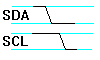
The start symbol is followed by transmission of the 7-bit slave address. This is necessary because multiple slaves can be connected to the same bus. The bits are transmitted one per SCLK cycle. The value can be changed during the low phase of SCLK and must remain stable during the high phase.
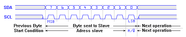
The bits are transmitted in big-endian order (most-significant bit first). After the seven bits of the address are transmitted, an eight read/write bit is transmitted. This should be 0 if the transmission is a write (master sending to slave) or 1 if the transmission is a read (master receiving from slave). In our case we will only be writing, so the read/write bit will always be 0.
After the address and read/write bit are sent, the master allows the SDAT line to float for one SCLK cycle. The slave whose address has just been transmitted should send an acknowledgement (ACK) by pulling SDAT low for the entire cycle.
After receiving the ACK, the master transmits the data a bit at a time in the same way it sent the address and read/write bit. After every eight bits, the master should wait one cycle for an ACK from the slave.
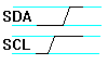
After the last byte is acknowledged by the slave, the master sends a STOP symbol to end the transmission by sending a low-to-high transition on SDAT while SCLK is held high.
If you look on page 17 of the SSM2603 datasheet, you will see that the codec takes 16-bit data words. Therefore, each transmission will have 3 acks (1 after address + r/w bit, 1 after each data byte) before a stop symbol must be sent. Another question which must be answered about the codec’s I2C interface is how fast SCLK can be toggled. If you look at page 5 of the datasheet, you will see that the maximum SCLK frequency is 526 kHz.
The I2C controller Verilog module looks like this.
module i2c_controller (
    input  clk,

    output i2c_sclk,
    inout  i2c_sdat,

    input  start,
    output done,
    output ack,

    input [23:0] i2c_data
);

reg [23:0] data;

reg [4:0] stage;
reg [6:0] sclk_divider;
reg clock_en = 1'b0;

// don't toggle the clock unless we're sending data
// clock will also be kept high when sending START and STOP symbols
assign i2c_sclk = (!clock_en) || sclk_divider[6];
wire midlow = (sclk_divider == 7'h1f);

reg sdat = 1'b1;
// rely on pull-up resistor to set SDAT high
assign i2c_sdat = (sdat) ? 1'bz : 1'b0;

reg [2:0] acks;

parameter LAST_STAGE = 5'd29;

assign ack = (acks == 3'b000);
assign done = (stage == LAST_STAGE);

always @(posedge clk) begin
    if (start) begin
        sclk_divider <= 7'd0;
        stage <= 5'd0;
        clock_en = 1'b0;
        sdat <= 1'b1;
        acks <= 3'b111;
        data <= i2c_data;
    end else begin
        if (sclk_divider == 7'd127) begin
            sclk_divider <= 7'd0;

            if (stage != LAST_STAGE)
                stage <= stage + 1'b1;

            case (stage)
                // after start
                5'd0:  clock_en <= 1'b1;
                // receive acks
                5'd9:  acks[0] <= i2c_sdat;
                5'd18: acks[1] <= i2c_sdat;
                5'd27: acks[2] <= i2c_sdat;
                // before stop
                5'd28: clock_en <= 1'b0;
            endcase
        end else
            sclk_divider <= sclk_divider + 1'b1;

        if (midlow) begin
            case (stage)
                // start
                5'd0:  sdat <= 1'b0;
                // byte 1
                5'd1:  sdat <= data[23];
                5'd2:  sdat <= data[22];
                5'd3:  sdat <= data[21];
                5'd4:  sdat <= data[20];
                5'd5:  sdat <= data[19];
                5'd6:  sdat <= data[18];
                5'd7:  sdat <= data[17];
                5'd8:  sdat <= data[16];
                // ack 1
                5'd9:  sdat <= 1'b1;
                // byte 2
                5'd10: sdat <= data[15];
                5'd11: sdat <= data[14];
                5'd12: sdat <= data[13];
                5'd13: sdat <= data[12];
                5'd14: sdat <= data[11];
                5'd15: sdat <= data[10];
                5'd16: sdat <= data[9];
                5'd17: sdat <= data[8];
                // ack 2
                5'd18: sdat <= 1'b1;
                // byte 3
                5'd19: sdat <= data[7];
                5'd20: sdat <= data[6];
                5'd21: sdat <= data[5];
                5'd22: sdat <= data[4];
                5'd23: sdat <= data[3];
                5'd24: sdat <= data[2];
                5'd25: sdat <= data[1];
                5'd26: sdat <= data[0];
                // ack 3
                5'd27: sdat <= 1'b1;
                // stop
                5'd28: sdat <= 1'b0;
                5'd29: sdat <= 1'b1;
            endcase
        end
    end
end

endmodule
SCLK is divided down by 128, giving us a frequency of about 390 kHz. The codec
steps through the bits one at a time, not checking the acks until all 24 bits
(7-bit address + r/w bit + 16-bit data) are transmitted. A transmission is
started when the start signal is set high, and done is set when the
transmission is complete. The ack signal is set high if all of the ACKs were
received. Another thing to note is that to set SDAT to high, we leave the
wire floating and rely on the pull-up resistor to pull the voltage
to a high value (z means high-impedance; assigning it to an inout signal
leaves the wire floating).
SSM2603 Register Settings
Now we have a way to send data through the configuration interface, but what data do we send? For that we must consult the datasheet. The first thing we need to know is what the slave address of the audio codec is. Page 17 of the datasheet states
If the CSB pin is set to 0, the address selected is 0011010; if 1, the address is 0011011
You can figure out what CSB is set to on the SoCKit by looking at the schematic. It’s actually a bit ambiguous in the schematic, which shows that CSB is connected to both Vdd and ground through resistors. However, the schematic helpfully notes that the default I2C address is 0x34 / 0x35. Note that this is an 8-bit word. The difference in the LSB refers to the read/write bit. Since we are only writing, the address we use is 0x34. This means CSB must be set to 0.
Now we need to figure out what the 16-bit data words are. The audio codec organizes its configuration variables into 19 9-bit registers. The first seven bits of the data transmission are the register address, and the last nine bits are the register contents.
The section on control register sequencing states
Enable all of the necessary power management bits of Register R6 with the exception of the out bit (Bit D4). The out bit should be set to 1 until the final step of the control register sequence.
We will be using all parts of the codec, so for now, set all of the bits in register 6 to 0 except bit 4.
Now let’s start from the top and work our way down.
Register 0 controls the input volume of the left channel ADC. We don’t want
simultaneous loading of volume, so set bit 8 to 0. We also don’t want mute,
so set bit 7 to 0 as well. Bits 5-0 specify the volume in decibels.
A decibel is a unit of signal power that operates on a logarithmic scale.
If a signal is specified as N dB, that means it is 10 N / 10
times more powerful than the baseline. You can specify any volume you want here,
but I suggest you just choose 0 dB (the baseline), which is 010111.
Choose the same options for the right-channel ADC control in register 1.
Registers 2 and 3 control left-channel and right-channel DAC volume, respectively. Put a 0 for bit 8, and set the volume to 0 dB, which is 1111001.
Register 4 contains options for the analog audio path. Bits 7-5 control the sidetone, which allows some of the microphone input to be mixed back to the output. This is used mainly in telephones because usability studies indicate that it is important feature. We will be feeding the microphone input back to the output anyway, so we do not need sidetone. Set the attenuation to 11, and the sidetone enable to 0. Bit 4 is the DAC select. We will be using the DAC, so set this to 1. Bits 3 and 2 control which input port (line input or microphone input) gets used as the input to the ADC. We want to use the microphone, so set the BYPASS to 0 and the INSEL to 1. Bit 1 is to mute the microphone, which we don’t want, so set this to 0. Bit 0 is MICBOOST, which controls the microphone amplifier. You can set this to either 0, for no boost, or 1, for 100x boost.
Register 5 controls the digital audio path. Bit 4 sets whether or not the DC offset is stored. We want the DC offset to be cleared, so set this to 0. Bit 3 is for digital mute, set this to 0. Bits 2-1 are for de-emphasis control, which helps improve the signal-to-noise ratio of the audio. Set these bits to 10, since we will be using a 44.1 kHz sampling rate. Bit 0 controls the ADC high pass filter. Set this to 0, the default.
Register 7 sets the options for the digital audio interface, which we will use to send and receive samples from the codec. We want the codec to run in left-justified slave mode with 16-bit samples. Set BCLKINV, MS, LRSWAP, and LRP to 0. Set WL to 00 for 16 bit audio, and set Format to 01 for left-justified mode. I will explain what all of these things mean in the next section.
Register 8 controls the sampling rate. We want a 44.1 kHz rate for both the ADC and the DAC. According to table 30 in the datasheet, this means we should set CLKODIV2 and CLKDIV2 to 0, SR to 1000, the base oversampling rate to 0, and USB mode select to 0.
Finally, we set register 6 to all zeros to power on the output and bit 0 of register 9 to 1 to activate the digital core.
Here is the final configuration controller. It steps through the different 16-bit data words for the I2C controller one at a time.
module i2c_av_config (
    input clk,
    input reset,

    output i2c_sclk,
    inout  i2c_sdat,

    output [3:0] status
);

reg [23:0] i2c_data;
reg [15:0] lut_data;
reg [3:0]  lut_index = 4'd0;

parameter LAST_INDEX = 4'ha;

reg  i2c_start = 1'b0;
wire i2c_done;
wire i2c_ack;

i2c_controller control (
    .clk (clk),
    .i2c_sclk (i2c_sclk),
    .i2c_sdat (i2c_sdat),
    .i2c_data (i2c_data),
    .start (i2c_start),
    .done (i2c_done),
    .ack (i2c_ack)
);

always @(*) begin
    case (lut_index)
        4'h0: lut_data <= 16'h0c10; // power on everything except out
        4'h1: lut_data <= 16'h0017; // left input
        4'h2: lut_data <= 16'h0217; // right input
        4'h3: lut_data <= 16'h0479; // left output
        4'h4: lut_data <= 16'h0679; // right output
        4'h5: lut_data <= 16'h08d4; // analog path
        4'h6: lut_data <= 16'h0a04; // digital path
        4'h7: lut_data <= 16'h0e01; // digital IF
        4'h8: lut_data <= 16'h1020; // sampling rate
        4'h9: lut_data <= 16'h0c00; // power on everything
        4'ha: lut_data <= 16'h1201; // activate
        default: lut_data <= 16'h0000;
    endcase
end

reg [1:0] control_state = 2'b00;

assign status = lut_index;

always @(posedge clk) begin
    if (reset) begin
        lut_index <= 4'd0;
        i2c_start <= 1'b0;
        control_state <= 2'b00;
    end else begin
        case (control_state)
            2'b00: begin
                i2c_start <= 1'b1;
                i2c_data <= {8'h34, lut_data};
                control_state <= 2'b01;
            end
            2'b01: begin
                i2c_start <= 1'b0;
                control_state <= 2'b10;
            end
            2'b10: if (i2c_done) begin
                if (i2c_ack) begin
                    if (lut_index == LAST_INDEX)
                        control_state <= 2'b11;
                    else begin
                        lut_index <= lut_index + 1'b1;
                        control_state <= 2'b00;
                    end
                end else
                    control_state <= 2'b00;
            end
        endcase
    end
end

endmodule
The Digital Audio Interface
Now that we have the audio codec configured, we need to implement a controller for the digital audio interface so that we can actually send samples to the DAC and receive samples from the ADC. In our configuration, we set the digital audio interface to left-justified slave mode. Slave mode simply means that the FPGA drives all of the clocks. There are five different clock signals and two data signals on the digital audio interface. The following table shows how the names for these signals in the FPGA settings file correspond to the names in the datasheet.
| FPGA Name | Datasheet Name | Type |
|---|---|---|
| AUD_ADCLRCK | RECLRC | Clock |
| AUD_ADCDAT | RECDAT | Data |
| AUD_DACLRCK | PBLRC | Clock |
| AUD_DACDAT | PBDAT | Data |
| AUD_XCK | MCLK | Clock |
| AUD_BCLK | BCLK | Clock |
You can figure this correspondence out for yourself by looking at the labels on the SoCKit schematic.
The Clocks
The first clock we have to worry about generating is the master clock MCLK. According to table 30, the frequency of this clock should be 11.2896 MHz. This frequency cannot be generated by simply dividing the master clock (there is no integer number N such that 50 / N is close enough to 11.2896). Fortunately, the Cyclone V contains specialty circuits called Phase-Locked Loops (PLLs) which can generate very precise clock signals. You can add a PLL to your design using Megawizard. The PLL megafunction is under “PLL” -> “Altera PLL v13.1”.
In the main page of the wizard, change the reference clock frequency to 50 MHz and uncheck the “Enable locked output port” option. In the “Output Clocks” section, change “Number of Clocks” to 2. We will use the PLL to generate a 11.2896 MHz clock for the audio codec and a 50 MHz main clock. Enter these frequencies in for “Desired Frequency”. For the 50 MHz clock, you will also need to change the actual frequency to the one right below 50 MHz (you can’t generate a clock faster than 50 MHz from a 50 MHz reference).
The next clock we have to consider is the bit clock, BCLK. According to table 30, this clock should be a quarter the frequency of the master clock. We can easily generate this using a frequency divider on the audio clock from the PLL.
The last two clocks are RECLRC and PBLRC. LRC stands for left right clock. This clock signals tells the codec which of the two stereo audio channels is being accessed. Since we chose not to invert the clocks, the two LRC signals are high for the left channel and low for the right channel. The frequency of these two clocks is 256 times slower than the master clock frequency. One cycle of LRC corresponds to a single audio frame. The clock division therefore makes sense, since 11.2896 MHz / 256 = 44.1 kHz. This signal is likewise generated by frequency division of the master audio clock.
Sending Data
The timing diagram on page 15 of the datasheet shows us how the data lines RECDAT and PBDAT are synchronized to the clocks. The data changes on each falling edge of BCLK. The first (most significant) bit of a sample is sent on the rising or falling edge of LRC.
You will notice that there are 128 / 4 = 32 cycles of BCLK in one phase of LRCK, but only 16 bits in a (mono) sample. Fortunately, the timing diagram shows us how to handle this. After transmitting the bits in big-endian order, the value of the data signals in the last 16 BCLK clocks cycles are don’t cares.
The Final Code
So here’s the final code for the audio codec driver. The clock passed in here
is the audio clock from the PLL, which is then divided down for LRC and BCLK.
The data is pushed out or read in through shift registers. There are also
sample_end and sample_req signals, which are asserted high for one cycle
after the last bit of an ADC sample is received or before the first bit of a
DAC sample must be sent.
module audio_codec (
    input  clk,
    input  reset,
    output [1:0]  sample_end,
    output [1:0]  sample_req,
    input  [15:0] audio_output,
    output [15:0] audio_input,
    // 1 - left, 0 - right
    input  [1:0] channel_sel,

    output AUD_ADCLRCK,
    input AUD_ADCDAT,
    output AUD_DACLRCK,
    output AUD_DACDAT,
    output AUD_BCLK
);

reg [7:0] lrck_divider;
reg [1:0] bclk_divider;

reg [15:0] shift_out;
reg [15:0] shift_temp;
reg [15:0] shift_in;

wire lrck = !lrck_divider[7];

assign AUD_ADCLRCK = lrck;
assign AUD_DACLRCK = lrck;
assign AUD_BCLK = bclk_divider[1];
assign AUD_DACDAT = shift_out[15];

always @(posedge clk) begin
    if (reset) begin
        lrck_divider <= 8'hff;
        bclk_divider <= 2'b11;
    end else begin
        lrck_divider <= lrck_divider + 1'b1;
        bclk_divider <= bclk_divider + 1'b1;
    end
end

assign sample_end[1] = (lrck_divider == 8'h40);
assign sample_end[0] = (lrck_divider == 8'hc0);
assign audio_input = shift_in;
assign sample_req[1] = (lrck_divider == 8'hfe);
assign sample_req[0] = (lrck_divider == 8'h7e);

wire clr_lrck = (lrck_divider == 8'h7f);
wire set_lrck = (lrck_divider == 8'hff);
// high right after bclk is set
wire set_bclk = (bclk_divider == 2'b10 && !lrck_divider[6]);
// high right before bclk is cleared
wire clr_bclk = (bclk_divider == 2'b11 && !lrck_divider[6]);

always @(posedge clk) begin
    if (reset) begin
        shift_out <= 16'h0;
        shift_in <= 16'h0;
        shift_in <= 16'h0;
    end else if (set_lrck || clr_lrck) begin
        // check if current channel is selected
        if (channel_sel[set_lrck]) begin
            shift_out <= audio_output;
            shift_temp <= audio_output;
            shift_in <= 16'h0;
        // repeat the sample from the other channel if not
        end else shift_out <= shift_temp;
    end else if (set_bclk == 1) begin
        // only read in if channel is selected
        if (channel_sel[lrck])
            shift_in <= {shift_in[14:0], AUD_ADCDAT};
    end else if (clr_bclk == 1) begin
        shift_out <= {shift_out[14:0], 1'b0};
    end
end

endmodule
You will notice that the AUD_XCK signal is missing here. That is because
we assign it at the top-level module directly from the PLL output.
module sockit_top (
    input  OSC_50_B8A,

    inout  AUD_ADCLRCK,
    input  AUD_ADCDAT,
    inout  AUD_DACLRCK,
    output AUD_DACDAT,
    output AUD_XCK,
    inout  AUD_BCLK,
    output AUD_I2C_SCLK,
    inout  AUD_I2C_SDAT,
    output AUD_MUTE,

    input  [3:0] KEY,
    input  [3:0] SW,
    output [3:0] LED
);

wire reset = !KEY[0];
wire main_clk;
wire audio_clk;

wire [1:0] sample_end;
wire [1:0] sample_req;
wire [15:0] audio_output;
wire [15:0] audio_input;

clock_pll pll (
    .refclk (OSC_50_B8A),
    .rst (reset),
    .outclk_0 (audio_clk),
    .outclk_1 (main_clk)
);

i2c_av_config av_config (
    .clk (main_clk),
    .reset (reset),
    .i2c_sclk (AUD_I2C_SCLK),
    .i2c_sdat (AUD_I2C_SDAT),
    .status (LED)
);

assign AUD_XCK = audio_clk;
assign AUD_MUTE = (SW != 4'b0);

audio_codec ac (
    .clk (audio_clk),
    .reset (reset),
    .sample_end (sample_end),
    .sample_req (sample_req),
    .audio_output (audio_output),
    .audio_input (audio_input),
    .channel_sel (2'b10),

    .AUD_ADCLRCK (AUD_ADCLRCK),
    .AUD_ADCDAT (AUD_ADCDAT),
    .AUD_DACLRCK (AUD_DACLRCK),
    .AUD_DACDAT (AUD_DACDAT),
    .AUD_BCLK (AUD_BCLK)
);

audio_effects ae (
    .clk (audio_clk),
    .sample_end (sample_end[1]),
    .sample_req (sample_req[1]),
    .audio_output (audio_output),
    .audio_input  (audio_input),
    .control (SW)
);

endmodule
Also at the top-level is the assignment for the AUD_MUTE signal. This signal
is active low, which means the codec is muted when AUD_MUTE is high.
Therefore, we set it so that it is only low when all the switches are off.
We’ve seen all of the modules included in this top-level except audio_effects,
which will hold all of our control logic. For now, audio_effects will just
contain some testing logic.
Testing it Out
Now that we have an audio codec controller, we should test that it can actually produce sound. To test the output, we can emit a fixed sine wave. The samples for this sine wave can be stored in a ROM. To test that the ADC is working, we can do straight feedback, sending samples coming in through the ADC back out through the DAC. We control what mode the control is in using the switches.
The sine wave we produce here is at 440 Hz. That is why there are 100 samples in our ROM, since one period of the sine wave contains 44100 / 440 = 100.2 samples.
module audio_effects (
    input  clk,
    input  sample_end,
    input  sample_req,
    output [15:0] audio_output,
    input  [15:0] audio_input,
    input  [3:0]  control
);

reg [15:0] romdata [0:99];
reg [6:0]  index = 7'd0;
reg [15:0] last_sample;
reg [15:0] dat;

assign audio_output = dat;

parameter SINE     = 0;
parameter FEEDBACK = 1;

initial begin
    romdata[0] = 16'h0000;
    romdata[1] = 16'h0805;
    romdata[2] = 16'h1002;
    romdata[3] = 16'h17ee;
    romdata[4] = 16'h1fc3;
    romdata[5] = 16'h2777;
    romdata[6] = 16'h2f04;
    romdata[7] = 16'h3662;
    romdata[8] = 16'h3d89;
    romdata[9] = 16'h4472;
    romdata[10] = 16'h4b16;
    romdata[11] = 16'h516f;
    romdata[12] = 16'h5776;
    romdata[13] = 16'h5d25;
    romdata[14] = 16'h6276;
    romdata[15] = 16'h6764;
    romdata[16] = 16'h6bea;
    romdata[17] = 16'h7004;
    romdata[18] = 16'h73ad;
    romdata[19] = 16'h76e1;
    romdata[20] = 16'h799e;
    romdata[21] = 16'h7be1;
    romdata[22] = 16'h7da7;
    romdata[23] = 16'h7eef;
    romdata[24] = 16'h7fb7;
    romdata[25] = 16'h7fff;
    romdata[26] = 16'h7fc6;
    romdata[27] = 16'h7f0c;
    romdata[28] = 16'h7dd3;
    romdata[29] = 16'h7c1b;
    romdata[30] = 16'h79e6;
    romdata[31] = 16'h7737;
    romdata[32] = 16'h7410;
    romdata[33] = 16'h7074;
    romdata[34] = 16'h6c67;
    romdata[35] = 16'h67ed;
    romdata[36] = 16'h630a;
    romdata[37] = 16'h5dc4;
    romdata[38] = 16'h5820;
    romdata[39] = 16'h5222;
    romdata[40] = 16'h4bd3;
    romdata[41] = 16'h4537;
    romdata[42] = 16'h3e55;
    romdata[43] = 16'h3735;
    romdata[44] = 16'h2fdd;
    romdata[45] = 16'h2855;
    romdata[46] = 16'h20a5;
    romdata[47] = 16'h18d3;
    romdata[48] = 16'h10e9;
    romdata[49] = 16'h08ee;
    romdata[50] = 16'h00e9;
    romdata[51] = 16'hf8e4;
    romdata[52] = 16'hf0e6;
    romdata[53] = 16'he8f7;
    romdata[54] = 16'he120;
    romdata[55] = 16'hd967;
    romdata[56] = 16'hd1d5;
    romdata[57] = 16'hca72;
    romdata[58] = 16'hc344;
    romdata[59] = 16'hbc54;
    romdata[60] = 16'hb5a7;
    romdata[61] = 16'haf46;
    romdata[62] = 16'ha935;
    romdata[63] = 16'ha37c;
    romdata[64] = 16'h9e20;
    romdata[65] = 16'h9926;
    romdata[66] = 16'h9494;
    romdata[67] = 16'h906e;
    romdata[68] = 16'h8cb8;
    romdata[69] = 16'h8976;
    romdata[70] = 16'h86ab;
    romdata[71] = 16'h845a;
    romdata[72] = 16'h8286;
    romdata[73] = 16'h8130;
    romdata[74] = 16'h8059;
    romdata[75] = 16'h8003;
    romdata[76] = 16'h802d;
    romdata[77] = 16'h80d8;
    romdata[78] = 16'h8203;
    romdata[79] = 16'h83ad;
    romdata[80] = 16'h85d3;
    romdata[81] = 16'h8875;
    romdata[82] = 16'h8b8f;
    romdata[83] = 16'h8f1d;
    romdata[84] = 16'h931e;
    romdata[85] = 16'h978c;
    romdata[86] = 16'h9c63;
    romdata[87] = 16'ha19e;
    romdata[88] = 16'ha738;
    romdata[89] = 16'had2b;
    romdata[90] = 16'hb372;
    romdata[91] = 16'hba05;
    romdata[92] = 16'hc0df;
    romdata[93] = 16'hc7f9;
    romdata[94] = 16'hcf4b;
    romdata[95] = 16'hd6ce;
    romdata[96] = 16'hde7a;
    romdata[97] = 16'he648;
    romdata[98] = 16'hee30;
    romdata[99] = 16'hf629;
end

always @(posedge clk) begin
    if (sample_end) begin
        last_sample <= audio_input;
    end

    if (sample_req) begin
        if (control[FEEDBACK])
            dat <= last_sample;
        else if (control[SINE]) begin
            dat <= romdata[index];
            if (index == 7'd99)
                index <= 7'd00;
            else
                index <= index + 1'b1;
        end else
            dat <= 16'd0;
    end
end

endmodule
To hear the results of the test hardware on the FPGA, plug your speakers into the green audio port on the FPGA and the microphone into the pink audio port. Flip switch 0 to hear the sine wave and switch 1 to hear the microphone feedback. If you are using headphones, I strongly suggest that you do not actually put then on, especially in the sine wave mode, as the volume at 0 dB is quite loud.
Conclusion
So now we have audio working on the FPGA. In my next post, I will discuss the implementation of FIR filters on the FPGA, which will allow us to do some interesting audio processing.